History of the LED
From a glowing crystal in 1907 to 200-lumen-per-watt solid-state lighting and MicroLED displays
The light-emitting diode took about 90 years to go from a lab curiosity to the world's main light source. Light from a semiconductor crystal was first seen in 1907. Practical infrared and red LEDs arrived in 1961–62. Yellow and brighter reds followed in the 1970s, the efficient blue LED in 1993 and the white LED in 1996. By the 2020s, LEDs made up more than half of global lighting sales.
The LED's story is not one invention but a relay race across physics, chemistry and manufacturing. A British radio engineer noticed the glow, a self-taught Soviet physicist explained it, American industrial labs turned it into products, and three Japanese researchers solved the problem that had defeated the industry for two decades: bright blue light. Each step unlocked a new color, and each new color unlocked new uses, from calculator displays and traffic signals to the screen you are reading this on.
Interactive timeline
The LED's history spans more than a century: H. J. Round saw light from carborundum in 1907, Holonyak made the first visible LED in 1962, the bright blue LED arrived in 1993 and the white LED in 1996, and LEDs passed half of global lighting sales in 2022. The timeline below covers each milestone.
Filter by era, or tap a year to jump straight to that milestone. Each entry links to the full section below.
- 1907H. J. Round sees light from carborundum
Working for Marconi, Round reports a yellowish glow from silicon carbide crystals under 10–110 V in Electrical World. It is the first published account of electroluminescence from a solid. Read more
- 1927Oleg Losev's papers and the "light relay" patent
Losev publishes a long series of papers showing the glow is not heat. He files a Soviet patent for using it to transmit signals, an early idea of optical telecommunication. Read more
- 1936Georges Destriau coins "electroluminescence"
In Paris, Destriau makes zinc sulfide powders glow in an alternating field and gives the phenomenon its name. Read more
- 1951The physics is explained
Kurt Lehovec and colleagues at the U.S. Army Signal Corps tie the SiC glow to carriers injected across a p–n junction, using the new semiconductor theory of the transistor era. Read more
- 1955Rubin Braunstein measures infrared from GaAs
At RCA, Braunstein reports infrared emission from gallium arsenide and other III–V alloys. In 1957 he shows the light can carry audio across a room. Read more
- 1961Biard & Pittman's infrared diode at Texas Instruments
While building GaAs tunnel diodes, the pair find strong 900 nm emission and patent the "semiconductor radiant diode". TI's SNX-100 (1962) becomes the first commercial LED. Read more
- 1962Nick Holonyak Jr. makes the first visible LED
At General Electric in Syracuse, Holonyak grows gallium arsenide phosphide and gets red light that people can see, for the first time from a practical semiconductor diode. Read more
- 1968Mass production begins
Monsanto starts high-volume production of red GaAsP LEDs. Hewlett-Packard uses them in numeric displays, and calculators and digital watches follow. Read more
- 1972M. George Craford: yellow, and 10× brighter red
At Monsanto, Holonyak's former student uses nitrogen-doped GaAsP to make the first yellow LED and red and orange LEDs about ten times brighter. Read more
- 1976Thomas P. Pearsall: LEDs for optical fiber
Pearsall engineers new semiconductor alloys whose emission matches the low-loss wavelengths of glass fiber, giving the first high-brightness, high-efficiency LEDs for telecommunications. Read more
- 1989Akasaki & Amano achieve p-type GaN
At Nagoya University, after perfecting crystal growth on a low-temperature buffer layer (1986), they make the first p-type gallium nitride and a GaN p–n junction LED. Read more
- 1993Shuji Nakamura's bright blue LED
At Nichia, Nakamura combines his two-flow MOCVD reactor, thermal annealing of p-GaN and InGaN active layers to produce a candela-class blue LED. Read more
- 1996The white LED
Nichia coats a blue InGaN chip with yellow cerium-doped YAG phosphor. The blue and yellow mix into white, the basis of almost every LED bulb today. Read more
- 1999The first high-power LED
Lumileds launches the 1 W Luxeon, with a heat-slug package that lets LEDs move from indicators to illumination. Read more
- 2007Phase-out laws begin
The U.S. Energy Independence and Security Act sets efficiency tiers for general-service lamps, and EU rules from 2009 start removing incandescent bulbs from shelves. Read more
- 2013OLED TVs and matrix headlights
LG sells the first large WOLED television, and Audi introduces Matrix LED headlights on the A8. Read more
- 2014Nobel Prize, and 303 lm/W in the lab
Akasaki, Amano and Nakamura receive the Nobel Prize in Physics. Cree reports a white LED at 303 lumens per watt. Read more
- 2018MicroLED goes modular
Samsung shows "The Wall", a modular MicroLED display, building on micro-LED arrays first reported by Jiang and Lin in 2000. Read more
- 2021Mini-LED goes mainstream
Mini-LED backlights with thousands of local-dimming zones arrive in tablets, laptops and mainstream TVs. Read more
- 2023The end of the incandescent era
A U.S. 45 lm/W minimum for general-service lamps takes full effect, and the EU ends most fluorescent lamps. LEDs now account for more than half of global lighting sales. Read more
1907: H. J. Round and the glowing carborundum
In 1907 Henry Joseph Round, an engineer working for Marconi, reported in Electrical World that carborundum (silicon carbide) crystal detectors glowed yellow, green, orange or blue when a voltage was applied. It was the first published observation of electroluminescence from a solid, though Round never pursued it.
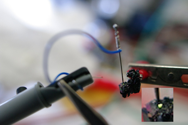

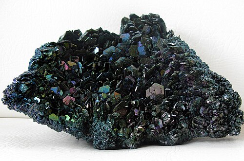
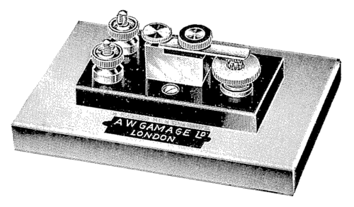
The first recorded observation of light from a solid-state electronic device came from Henry Joseph Round, a British engineer and assistant to Guglielmo Marconi. In the early 1900s, radio receivers used crystal detectors to rectify radio signals. These were small mineral crystals touched by a fine metal wire, the cat's whisker. One of the most popular crystals was carborundum, or silicon carbide (SiC), an industrial abrasive that happened to be a semiconductor.
While testing carborundum detectors, Round noticed that some crystals gave off light when a voltage was applied across the point contact. In February 1907 he described it in a short letter to the journal Electrical World, titled "A Note on Carborundum." He reported a yellowish glow at 10 V, and green, orange and blue glows from other crystals at voltages up to 110 V. He noted that the light seemed to come from the contact point, and in some crystals only from the edges.
Round did not pursue the effect, and the note was largely forgotten for decades. It still matters because it fixes the starting point of LED history. It shows that electroluminescence comes from the semiconductor material itself, not from a heated filament or a gas discharge. Silicon carbide came back eighty years later as a substrate for blue LEDs, and today it is a leading material for power electronics.


1920s: Oleg Losev, the forgotten pioneer
Oleg Losev, a self-taught Soviet radio physicist, published about sixteen papers between 1924 and 1930 proving that the glow from carborundum detectors was not heat and came from a thin active layer. In 1927 he applied for a patent on a "light relay" for optical signalling. He died in the Siege of Leningrad in 1942.
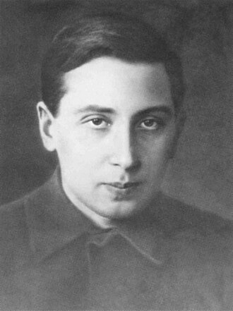

Oleg Vladimirovich Losev (1903–1942) had no university degree, but he became one of the most original experimental physicists of early Soviet radio. Working at the Nizhny Novgorod Radio Laboratory in the early 1920s, he first became known for the "crystadyne". It used the negative resistance of a biased zincite crystal to amplify and generate radio signals, decades before the tunnel diode.
From about 1923, Losev studied the same glow that Round had seen in carborundum detectors, and he went much further. Between 1924 and 1930 he published about sixteen papers in Russian, German and British journals that carefully characterized what later writers called "Losev light." He showed that:
- the light appeared at very low voltages and switched on and off almost instantly, so it could not be incandescence (heat glow);
- light came from a thin active layer near the surface of the crystal, matching what we now call the junction region;
- the emission spectrum depended on the crystal, not on the metal contact.
Losev described the effect as the inverse of the photoelectric effect, which Einstein had explained in 1905. That was remarkably close to the modern explanation. In 1927 he applied for a Soviet patent on a "light relay", which used the fast-switching glow of a crystal detector to transmit telegraph and telephone signals as light. It was one of the first proposals for optical telecommunication using a semiconductor emitter. He also studied the reverse process, photovoltaic effects in SiC, and anticipated parts of solar-cell physics.
His work stopped tragically early. Losev died of starvation in January 1942 during the Siege of Leningrad, aged 38. Because most of his papers were in Russian and the theory needed to explain them (band theory and the p–n junction) did not yet exist, his work stayed obscure in the West. Historians rediscovered it in the 1990s and 2000s, and he is now widely recognized as the true founder of LED science.
1930s–1950s: Naming and explaining the glow
In 1936 Georges Destriau made zinc sulfide powders glow in an alternating field and coined the word electroluminescence. The explanation came with transistor-era semiconductor theory: in 1951 Kurt Lehovec and colleagues showed the light comes from carriers injected across a p–n junction that recombine and emit photons.
In 1936 the French physicist Georges Destriau, working in Marie Curie's former laboratory in Paris, made zinc sulfide (ZnS) powders glow by suspending them in an insulating medium and applying a strong alternating electric field. He coined the term electroluminescence for light produced directly by an electric field in a material. Destriau's powder devices led to electroluminescent (EL) panels, which appeared in night lights, instrument backlights and later the green EL displays of early laptops. These are a cousin of the LED, not the same device.
The theory that finally explained Round's and Losev's observations came from the push to understand semiconductors that led to the transistor at Bell Labs in 1947. Band theory, the idea of electrons and "holes" as charge carriers, and William Shockley's theory of the p–n junction gave physicists the vocabulary they needed. In 1951 Kurt Lehovec, Carl Accardo and Edward Jamgochian at the U.S. Army Signal Corps Engineering Laboratories published an analysis of light from SiC junctions. They attributed it to minority carriers injected across a p–n junction that recombine and release their energy as photons. That is still the core of how every LED works (see How LEDs work).
1955–1962: Infrared LEDs from gallium arsenide
Practical LEDs began with gallium arsenide, a direct-bandgap III–V semiconductor that emits infrared light efficiently. Rubin Braunstein reported GaAs emission at RCA in 1955, and in 1961 James Biard and Gary Pittman at Texas Instruments found strong infrared emission from GaAs diodes and patented the device, which TI sold from 1962 as the SNX-100, the first commercial LED.
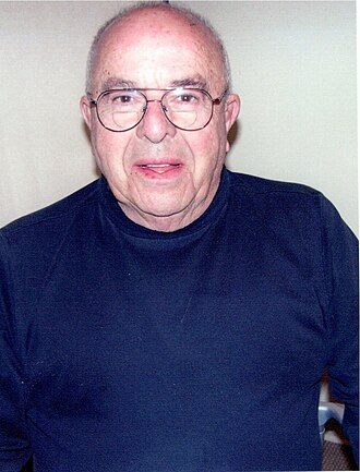

Silicon carbide's glow was faint because SiC is an indirect-bandgap semiconductor. Electrons and holes in it rarely recombine by emitting light. The breakthrough came from a new family of materials: the III–V compound semiconductors, made by combining elements from groups III (gallium, indium, aluminium) and V (arsenic, phosphorus, nitrogen) of the periodic table. Many of them, above all gallium arsenide (GaAs), have a direct bandgap, so recombination produces light efficiently.
Rubin Braunstein at RCA (1955–1957)
In 1955 Rubin Braunstein of RCA reported infrared light from simple diodes of gallium arsenide, gallium antimonide, indium phosphide and silicon-germanium. In 1957 he used a GaAs emitter to send music from a record player to a nearby detector, an early demonstration of optical communication with LEDs.
In 1955 Rubin Braunstein of the Radio Corporation of America reported infrared emission from simple diodes made of GaAs, gallium antimonide (GaSb), indium phosphide (InP) and silicon-germanium alloys, at room temperature and at 77 K. In 1957 he showed that the light could carry information. He used a GaAs emitter to send an audio signal from a record player to a detector a short distance away, a small-scale preview of optical communication.
James Biard and Gary Pittman at Texas Instruments (1961)
In 1961 James Biard and Gary Pittman were building gallium arsenide tunnel diodes at Texas Instruments when an infrared microscope showed them glowing at about 900 nm. Their 1962 "Semiconductor Radiant Diode" patent, granted in 1966, is widely regarded as the first patent for a practical LED.
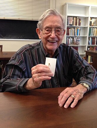

In 1961 James R. Biard and Gary Pittman were trying to build GaAs tunnel diodes at Texas Instruments in Dallas. Using a newly acquired infrared microscope, they saw that their diodes emitted strong near-infrared light, around 900 nm, when forward biased. They recognized its value and filed a patent for a "Semiconductor Radiant Diode" in 1962. It was granted in 1966 as U.S. Patent 3,293,513, and it is widely regarded as the first patent for a practical LED.
In October 1962 TI launched the SNX-100, a GaAs infrared LED at about 890 nm, the first commercial LED product. It sold for about $130. The first customers were not consumers but defense and industrial users, who paired the LED with photodetectors for optical isolators, punched-card readers and early sensing systems. Infrared LEDs are still produced in enormous numbers for remote controls, optocouplers and sensors (see Infrared LEDs).
1962: Nick Holonyak Jr. and the first visible LED
On 9 October 1962 Nick Holonyak Jr. at General Electric made the first practical visible LED. By alloying gallium arsenide with gallium phosphide into GaAsP, he widened the band gap enough to emit red light near 650–700 nm while keeping it direct. He is often called the father of the LED.
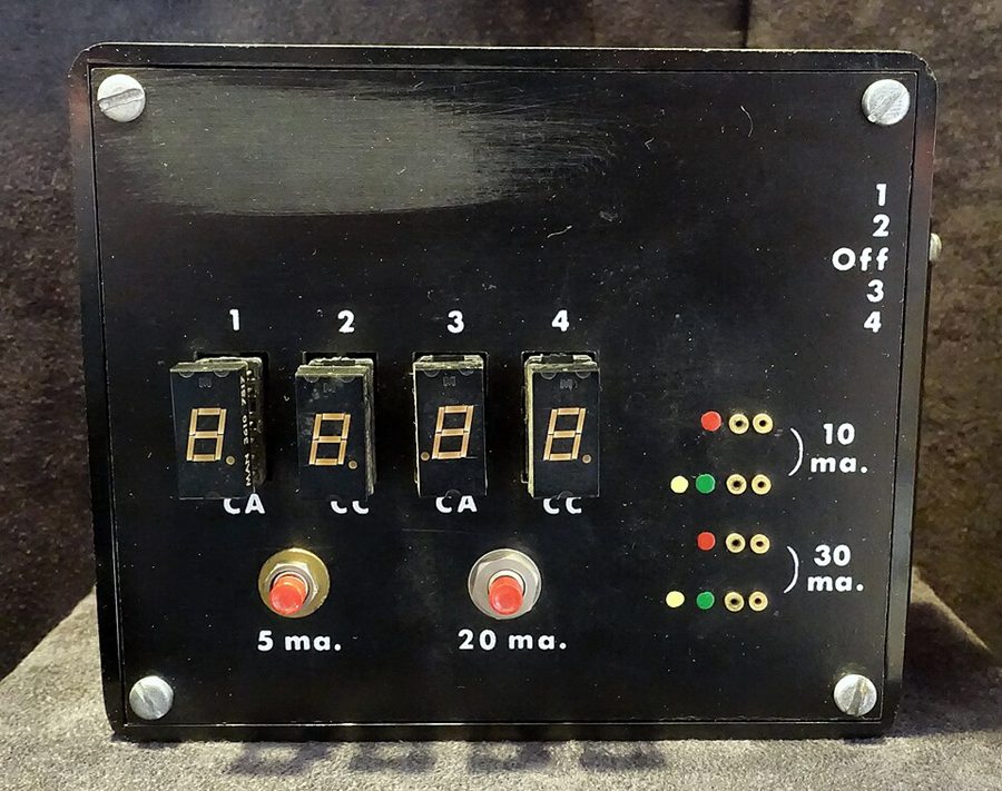

Infrared light is invisible, so the LEDs of 1961 were useless as indicators or displays. Nick Holonyak Jr., a consulting scientist at General Electric's Advanced Semiconductor Laboratory in Syracuse, New York, set out to make a semiconductor that emitted visible light. He had been the first graduate student of John Bardeen, co-inventor of the transistor.
His insight was to alloy gallium arsenide with gallium phosphide. GaAs emits infrared around 870 nm. GaP has a wider bandgap, but it is indirect and a poor emitter. By growing gallium arsenide phosphide (GaAs1−xPx) with the right phosphorus fraction, Holonyak widened the bandgap enough to push emission into the red, near 650–700 nm, while keeping it direct. Many colleagues doubted that a mixed crystal could be grown with good enough quality. Holonyak used vapor-phase methods to grow it anyway.
On 9 October 1962 his GaAsP junctions produced red light, both as an LED and, in suitably shaped samples, as a visible semiconductor laser. The results appeared in Applied Physics Letters that December. This was the first practical visible-spectrum LED, and Holonyak predicted it would one day replace the incandescent bulb, a claim that took fifty years to come true.
Holonyak moved to the University of Illinois at Urbana-Champaign in 1963. There he trained generations of optoelectronics researchers and later helped develop quantum-well lasers and the transistor laser. His honors included the National Medal of Science, the National Medal of Technology, the Japan Prize and the Draper Prize. He died in 2022 at the age of 93.
1968–1980s: LEDs become products
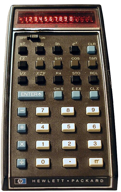
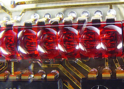
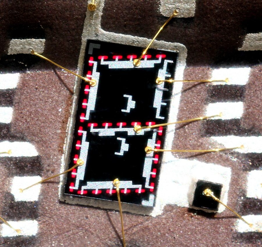
Monsanto began mass-producing red GaAsP LEDs in 1968 and supplied Hewlett-Packard, which used them in instrument displays and, from 1972, pocket calculators. Prices fell from hundreds of dollars to cents, and LEDs became the standard indicator light and the glowing digits of early calculators and digital watches.
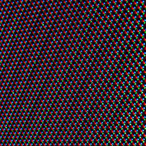

Early visible LEDs were expensive, dim (a few millicandelas) and made one at a time. Industrialization came from Monsanto, the chemical company, which had the expertise in high-purity materials to grow GaAsP wafers in volume. In 1968 Monsanto became the first company to mass-produce visible LEDs. It supplied red GaAsP chips to Hewlett-Packard, which built them into small numeric displays for its instruments and, from 1972, its pocket calculators.
Prices fell from hundreds of dollars to a few cents per LED during the 1970s. Red LEDs became the default indicator light on radios, stereos and test equipment. They also formed the glowing seven-segment digits of calculators and the first digital watches, such as the Hamilton Pulsar of 1972. Those watches had to be pressed to light up because the LEDs drained the battery quickly. In the late 1970s, liquid-crystal displays, which drew far less power, replaced LEDs in watches and calculators. LEDs kept the indicator market and moved into new applications such as alphanumeric signs, optocouplers and remote controls.



1972: M. George Craford's yellow LED
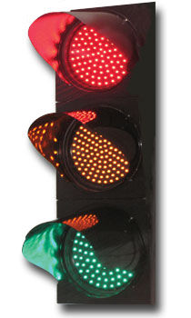
In 1972 M. George Craford, a former student of Holonyak working at Monsanto, doped GaAsP with nitrogen to make the first yellow LED and red and orange LEDs about ten times brighter. He later led Hewlett-Packard's AlInGaP work, which made LED traffic signals and tail lights practical.

M. George Craford, a former graduate student of Holonyak, joined Monsanto and in 1972 made two advances. By doping GaAsP with nitrogen, which creates "isoelectronic traps" that help electrons and holes recombine radiatively even in the indirect-bandgap part of the alloy range, he produced the first yellow LED. The same technique made red and red-orange LEDs about ten times brighter.
Craford later moved to Hewlett-Packard and then Lumileds. There he led the development of AlInGaP (aluminium indium gallium phosphide) LEDs in the 1990s, which brought red, orange and amber LEDs to brightness levels good enough for traffic signals and automotive tail lights. He received the U.S. National Medal of Technology in 2002.
1976: Thomas P. Pearsall and fiber-optic LEDs
In 1976 Thomas P. Pearsall engineered indium gallium arsenide phosphide alloys whose emission matched the low-loss wavelengths of glass fiber, around 1.3 and 1.55 micrometers. These high-brightness infrared LEDs powered the first generation of fiber-optic links and remained in short-reach networks, such as 100BASE-FX Ethernet, for decades.
By the mid-1970s, low-loss glass optical fiber had become practical. Fiber attenuates light least in the near-infrared, roughly around 1.3 µm and 1.55 µm, well beyond what GaAs emits. In 1976 Thomas P. Pearsall created high-brightness, high-efficiency LEDs for fiber-optic telecommunications by engineering new semiconductor alloys (the indium gallium arsenide phosphide family, grown on indium phosphide) whose bandgap matched those transmission wavelengths.
LEDs were the light source of the first generation of fiber systems and stayed in use for short-reach multimode links for decades. 100BASE-FX Ethernet, for example, used 1300 nm LEDs. Lasers took over long-haul links because their narrow spectrum and high power travel further. Pearsall's materials work also laid groundwork for the photodetectors and lasers used throughout the optical internet (see Telecom & sensing).
1980s–1990s: The brightness race
Through the 1980s, AlGaAs heterostructures produced "superbright" red LEDs readable in daylight. In the early 1990s, AlInGaP from Hewlett-Packard and Toshiba brought efficient red, orange, amber and yellow, beating filtered incandescent lamps, so traffic signals and tail lights switched to LEDs. Efficient blue was still missing.
Through the 1980s, LED efficiency rose steadily, roughly following what would later be called Haitz's law. Aluminium gallium arsenide (AlGaAs) heterostructure LEDs gave "superbright" reds that could be read in daylight and were used in signs, high-mounted brake lights and early message boards. Heterostructures sandwich a thin, narrow-bandgap active layer between wider-bandgap layers so that carriers are confined where they can recombine.
The decisive step for red, orange, amber and yellow came in the early 1990s with AlInGaP, commercialized by Hewlett-Packard and Toshiba. HP's transparent-substrate AlInGaP LEDs of the mid-1990s were, for the first time, more efficient than filtered incandescent lamps of the same color. Red traffic signals and car tail lights were the first big lighting markets to switch. An incandescent red traffic signal throws away most of its light in the red filter, while a red LED makes only the needed color. An LED signal head drew about 10–15 W instead of 70–150 W and lasted years instead of months.
Blue was still missing. Without an efficient blue emitter there was no full-color LED display and no white LED. The blue devices of the time were made of silicon carbide (sold by Cree from 1989) and were extremely inefficient. Zinc selenide devices were bright but burned out in hours.
1989–1996: The blue LED and white light
Gallium nitride had the right band gap for blue light, but it could not be grown as good crystals and nobody could make p-type GaN. Akasaki and Amano solved both problems between 1986 and 1989, and Shuji Nakamura at Nichia made the process manufacturable, launching a bright InGaN blue LED in 1993.
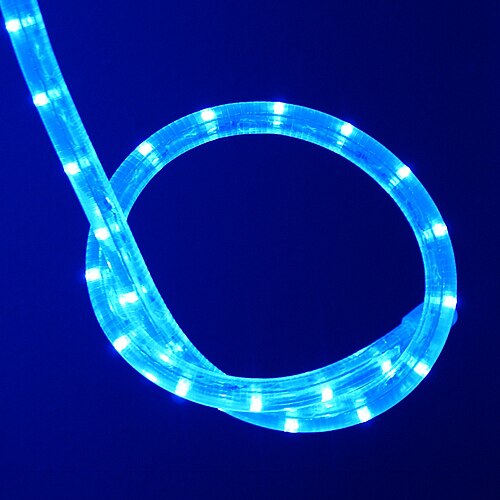

Gallium nitride (GaN) had the right properties on paper: a direct bandgap of about 3.4 eV (near-ultraviolet) that could be lowered into the blue and green by alloying with indium. In practice it seemed impossible to work with. No GaN substrate existed, so crystals had to be grown on sapphire, whose atomic spacing differs by about 16%, which produced films full of cracks and defects. Worse, nobody could make p-type GaN, the hole-rich half of the junction. In 1972 Herbert Paul Maruska at RCA demonstrated a violet GaN emitter, but without p-type material it was dim and unreliable. Most of the industry abandoned GaN in favor of zinc selenide.
Isamu Akasaki and Hiroshi Amano (Nagoya University)
At Nagoya University, Isamu Akasaki and his student Hiroshi Amano grew high-quality GaN on sapphire in 1986 using a low-temperature aluminum nitride buffer layer. In 1989 they made magnesium-doped GaN truly p-type with electron-beam treatment and built the first GaN p–n junction LED, emitting ultraviolet and blue light.
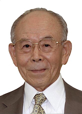

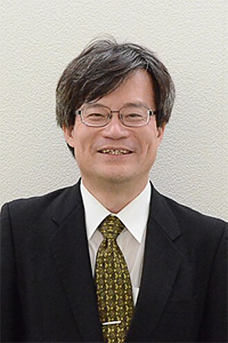

Isamu Akasaki kept working on GaN for decades after most others had given up. At Nagoya University, he and his graduate student Hiroshi Amano made two breakthroughs. In 1986, they grew smooth, high-quality GaN on sapphire by first depositing a thin low-temperature aluminium nitride buffer layer using metal-organic vapor phase epitaxy (MOVPE). The buffer absorbed the lattice mismatch. In 1989 they discovered that magnesium-doped GaN became genuinely p-type after treatment with a low-energy electron beam (LEEBI). That allowed them to build the first GaN p–n junction LED, which emitted ultraviolet and blue light.
Shuji Nakamura (Nichia Corporation)
Shuji Nakamura, an engineer at the small Japanese phosphor maker Nichia, built a two-flow MOCVD reactor, discovered that thermal annealing activates p-type GaN across whole wafers, and grew bright InGaN layers. Nichia's candela-class blue LED of 1993 was about 100 times brighter than earlier blue LEDs.


Shuji Nakamura was an engineer at Nichia, a small phosphor maker on the island of Shikoku with no track record in LEDs. He persuaded the company's founder to fund a GaN effort and largely built his equipment himself. His two-flow MOCVD reactor (1991) used a second gas stream to press the reactant flow onto the hot substrate, giving very uniform GaN. In 1992 he found that simply annealing Mg-doped GaN in a hydrogen-free atmosphere activated p-type conduction on a whole wafer. He showed that hydrogen from the growth process had been passivating the magnesium, which explained why p-type GaN had been so elusive.
Nakamura then grew high-quality indium gallium nitride (InGaN) active layers, whose bandgap could be tuned from ultraviolet into blue and green. In November 1993 Nichia announced a candela-class blue LED, roughly 100 times brighter than the SiC blue LEDs on the market. Bright green InGaN LEDs followed in 1995, completing the RGB set needed for full-color LED screens, and a blue-violet laser diode in 1996 led directly to the Blu-ray Disc. Nakamura joined the University of California, Santa Barbara in 1999. A long legal dispute over his compensation for the invention became a landmark in Japanese employee-invention law.
1996: The first white LED
In 1996 Nichia coated a blue InGaN chip with yellow cerium-doped YAG phosphor. The phosphor converts part of the blue light to a broad yellow band, and the mix looks white. Early versions were bluish and made only about 5 lumens per watt, but almost every white LED still uses this principle.
With blue in hand, Nichia made the device that would transform lighting. In 1996 it coated a blue InGaN chip with cerium-doped yttrium aluminium garnet (YAG:Ce), a phosphor the company knew well. The phosphor absorbs part of the blue light and re-emits a broad band of yellow. The remaining blue plus the yellow is perceived as white. Early white LEDs had a cold, bluish tint and efficacies of only a few lumens per watt. The architecture proved endlessly improvable, though, and nearly every white LED made today uses the same principle with refined chips and phosphor blends (see Making white light).
2014: The Nobel Prize in Physics
In 2014 Isamu Akasaki, Hiroshi Amano and Shuji Nakamura shared the Nobel Prize in Physics "for the invention of efficient blue light-emitting diodes which has enabled bright and energy-saving white light sources." The committee stressed that without blue LEDs, white LED lighting would have been impossible.
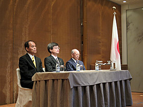

On 7 October 2014 the Royal Swedish Academy of Sciences awarded the Nobel Prize in Physics jointly to Isamu Akasaki, Hiroshi Amano and Shuji Nakamura "for the invention of efficient blue light-emitting diodes which has enabled bright and energy-saving white light sources." The committee noted that red and green LEDs had existed for decades, but that without blue, white LED lamps were impossible. It also noted that LED lighting could greatly reduce the share of world electricity used for lighting, then about one-fifth of the total. It was an unusual Nobel for a device invented so recently that it was still changing the world while the prize was awarded.
2000s–today: The solid-state lighting revolution
White LEDs moved into general lighting after Lumileds launched the 1-watt Luxeon in 1999. Haitz's law, a tenfold fall in cost per lumen and twentyfold rise in output per package each decade, held for over twenty years. Efficacy rose from about 5 lm/W in 1996 to a laboratory record of 303 lm/W in 2014.
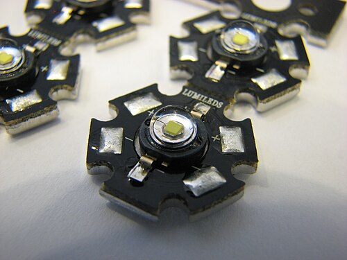

Once white LEDs existed, the race was on to make them bright and cheap enough for general lighting. In 1999 Lumileds introduced the 1-watt Luxeon, the first true high-power LED. It mounted the chip on a heat slug so it could run at 350 mA instead of 20 mA. Cree's XLamp family (2006 onward) and many competitors followed. In 2000 Roland Haitz of Agilent described the trend that bears his name: every decade, the cost per lumen falls by a factor of 10 and the light output per LED package rises by a factor of 20. The prediction held for more than twenty years.
| Year | Milestone | Efficacy |
|---|---|---|
| 1996 | First commercial white LED (Nichia) | ~5 lm/W |
| 2002 | High-power white parts beat incandescent | ~25 lm/W |
| 2006 | Laboratory record passes 100 lm/W | ~130 lm/W |
| 2011 | Philips wins the U.S. DOE L Prize with a 10 W, ~900 lm "60 W" replacement | ~90 lm/W (lamp) |
| 2014 | Cree laboratory record | 303 lm/W |
| 2020s | Mainstream mid-power packages at nominal current | 200–230 lm/W |
Phase-outs of incandescent and fluorescent lighting
Governments accelerated the switch to LEDs. The EU removed incandescent bulbs between 2009 and 2012 and most fluorescent lamps in 2023, while a U.S. minimum of 45 lumens per watt ended sales of incandescent and halogen household bulbs in 2023. A 2024 U.S. rule raises the minimum to roughly 120 lm/W from 2028.
Governments sped up the transition. Australia announced an incandescent phase-out in 2007. The U.S. Energy Independence and Security Act of 2007 set efficiency tiers for general-service lamps from 2012 to 2014. The EU withdrew incandescent bulbs in stages from 2009 to 2012 and non-directional halogen lamps in 2018. In the United States a minimum of 45 lumens per watt for general-service lamps took full effect in 2023, which effectively ended sales of incandescent and halogen household bulbs. A further Department of Energy rule finalized in 2024 raises the minimum for most general-service lamps to roughly 120 lm/W from 2028, a level only LEDs can meet. In 2023 the EU also ended most compact and linear fluorescent lamps under its mercury restrictions. According to the International Energy Agency, LEDs passed 50% of global lighting sales in 2022.
LEDs take over screens: OLED, QLED, Mini-LED and MicroLED
LEDs also took over screens. Kodak's 1987 OLED research led to AMOLED phones and, from 2013, large OLED TVs. LCDs answered with quantum-dot "QLED" films from about 2015 and Mini-LED backlights from 2019, while MicroLED, where every sub-pixel is its own inorganic LED, appeared in Samsung's The Wall in 2018.
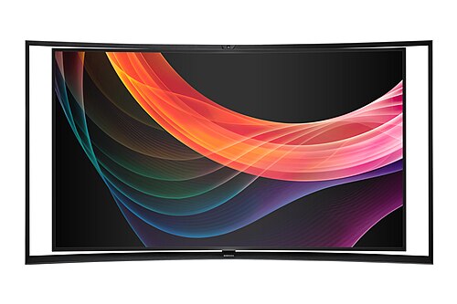

In parallel, LEDs transformed displays. Organic LEDs (OLEDs) date to the 1987 work of Ching Tang and Steven Van Slyke at Eastman Kodak. Sony sold the first OLED TV, the 11-inch XEL-1, in 2007. AMOLED screens became standard on flagship smartphones in the 2010s, and LG launched large white-OLED (WOLED) televisions in 2013. Samsung Display added QD-OLED, blue OLED with quantum-dot color conversion, in 2022.
LCDs kept improving by changing their LED backlights. Quantum-dot enhancement films, marketed as "QLED", widened color gamut from about 2015. Mini-LED backlights with thousands of tiny LEDs and hundreds to thousands of local-dimming zones appeared in TVs from 2019 and in tablets and laptops from 2021. At the frontier is MicroLED, in which every sub-pixel is its own microscopic inorganic LED. Hongxing Jiang and Jingyu Lin demonstrated micro-LED arrays in 2000, Samsung showed its modular MicroLED "The Wall" in 2018, and the race to mass-produce MicroLED for watches, AR glasses and TVs continues (see MicroLED).
LEDs have also changed architecture and entertainment. Stadiums now switch instantly between game lighting and light shows. Cities have replaced orange sodium streetlights with LEDs. The Las Vegas Sphere, opened in 2023, wraps a building in about 1.2 million LED pucks.
The 2020s: the MicroLED era begins
In the 2020s the frontier moved to MicroLED displays, in which every sub-pixel is an inorganic LED usually under 50 µm. Samsung and LG sell hand-built luxury MicroLED screens, but mass transfer of millions of tiny dies and inefficient red micro-LEDs keep costs high. Watches, cars and AR glasses will likely come first.
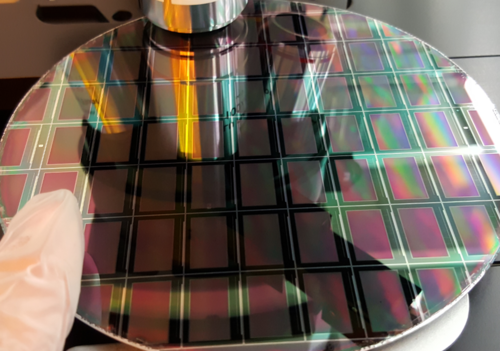

Sixty years after Holonyak's red LED, the frontier moved from lighting back to displays. In MicroLED screens every red, green and blue sub-pixel is its own inorganic LED, usually smaller than 50 µm. The idea grew out of the micro-LED arrays demonstrated by Hongxing Jiang and Jingyu Lin in 2000. Samsung showed the modular 146-inch "The Wall" in 2018 and sold a 110-inch MicroLED TV from 2021, and LG introduced its MAGNIT MicroLED displays in the early 2020s. All of them are hand-built luxury products whose prices run to six figures.
The obstacle is manufacturing rather than physics. A 4K panel needs about 25 million working LEDs, which must be grown, tested, moved by mass transfer and repaired with near-perfect yield. Red micro-LEDs also lose efficiency as they shrink. In 2024, reports that Apple had shelved its MicroLED smartwatch program showed how hard the economics remain. Meanwhile, two related technologies reached mass markets. Mini-LED backlights with thousands of dimming zones spread through tablets, laptops and TVs from 2021, and monolithic MicroLED microdisplays, grown on silicon wafers, began shipping in augmented-reality glasses. Most researchers expect MicroLED to reach watches, cars and AR headsets before living rooms (see OLED vs QLED vs Mini-LED vs MicroLED).
What comes next
Research is now focused on closing the "green gap" between 530 and 590 nm, reducing efficiency droop at high currents, improving deep-UV LEDs for disinfection, and mass-producing MicroLED screens. New emitters such as perovskite and quantum-dot LEDs, and Li-Fi networking through LED lights, could open the next chapter.
The LED's history is not finished. Current research areas include:
- Closing the "green gap". InGaN and AlInGaP are both inefficient between about 530 and 590 nm. Efficient direct green and amber emitters would allow RGB lighting that beats phosphor-converted white.
- Efficiency droop. LED efficiency falls at high current densities, largely because of Auger recombination. Solving it would allow fewer, smaller chips per lumen.
- Deep-UV LEDs. AlGaN UV-C LEDs are replacing mercury lamps for disinfection, but their wall-plug efficiency is still in the single digits.
- MicroLED manufacturing. Mass transfer of tens of millions of micro-dies, and efficient red micro-emitters, are the main obstacles to affordable MicroLED screens.
- New emitters. Perovskite LEDs, quantum-dot electroluminescence (true "QD-LEDs") and nanowire LEDs could change displays again.
- Light as a network. Visible-light communication, standardized as IEEE 802.11bb ("Li-Fi") in 2023, turns LED luminaires into data access points.
Frequently asked questions
Who invented the LED?
No single person. H. J. Round first observed the effect (1907), Oleg Losev studied and patented it (1920s), James Biard and Gary Pittman patented the first practical infrared LED at Texas Instruments (1961–62), and Nick Holonyak Jr. made the first visible red LED at GE (1962). Holonyak is usually called the father of the LED.
When was the first LED sold?
Texas Instruments' SNX-100 infrared LED went on sale in October 1962. Visible red LEDs went into mass production at Monsanto in 1968.
Why did it take so long to make a blue LED?
The best candidate material, gallium nitride, could not be grown as good crystals, and no one could make p-type GaN. Akasaki and Amano solved crystal growth (1986) and p-type doping (1989). Nakamura made the process manufacturable and added InGaN to get bright blue (1993).
When did white LEDs appear?
Nichia introduced the first white LED in 1996 by coating a blue InGaN chip with yellow YAG:Ce phosphor.
When did LED bulbs replace incandescent bulbs?
LED household bulbs became affordable around 2012–2015. Regulations completed the switch: the EU phased out incandescent lamps from 2009 to 2012 and halogens in 2018, and the U.S. 45 lm/W rule took effect in 2023.
Sources and further reading
- H. J. Round, "A Note on Carborundum," Electrical World 49, 309 (1907).
- N. Zheludev, "The life and times of the LED — a 100-year history," Nature Photonics 1, 189–192 (2007).
- K. Lehovec, C. A. Accardo, E. Jamgochian, "Injected light emission of silicon carbide crystals," Physical Review 83, 603 (1951).
- R. Braunstein, "Radiative transitions in semiconductors," Physical Review 99, 1892 (1955).
- J. R. Biard, G. E. Pittman, "Semiconductor radiant diode," U.S. Patent 3,293,513 (1966).
- N. Holonyak Jr., S. F. Bevacqua, "Coherent (visible) light emission from Ga(As1−xPx) junctions," Applied Physics Letters 1, 82 (1962).
- The Royal Swedish Academy of Sciences, "Efficient blue light-emitting diodes leading to bright and energy-saving white light sources," Scientific Background on the Nobel Prize in Physics 2014.
- S. Nakamura, T. Mukai, M. Senoh, "Candela-class high-brightness InGaN/AlGaN double-heterostructure blue-light-emitting diodes," Applied Physics Letters 64, 1687 (1994).
- R. Haitz, F. Kish, J. Tsao, J. Nelson, "The case for a national research program on semiconductor lighting," Sandia/Agilent white paper (2000).
- U.S. Department of Energy, Solid-State Lighting Program, and IEA, "Lighting" tracking report (2023).
- U.S. Department of Energy (DOE), "Energy Conservation Program: Energy Conservation Standards for General Service Lamps," final rule (2024).
- S. X. Jin, J. Li, J. Z. Li, J. Y. Lin, H. X. Jiang, "GaN microdisk light emitting diodes," Applied Physics Letters 76, 631 (2000).
Image credits
- Nick Holonyak Jr.: unknown author, public domain (Wikimedia Commons).
- Oleg Losev: unknown author, public domain (Wikimedia Commons).
- Rubin Braunstein: Bagelverse, CC BY-SA 4.0.
- James R. Biard: Gymnstx64, CC BY-SA 4.0.
- Isamu Akasaki: Government of Japan, CC BY 4.0. Hiroshi Amano and Shuji Nakamura: Ministry of Education, Culture, Sports, Science and Technology (MEXT), Japan, CC BY 4.0. Nobel laureates in Stockholm: Embassy of Japan in Sweden, CC BY 4.0.
- Replica of Round's 1907 experiment: Biolippi, CC BY-SA 3.0. Holonyak's LED demonstration box at the Spurlock Museum: Daderot, public domain. Canon LE-10 seven-segment LED die: Mister rf, CC BY-SA 4.0.
- LED display: Martin Kraft, CC BY-SA 3.0. Blue LEDs: Hi-Res Images of Chemical Elements, CC BY 3.0. OLED TV: Samsung Belgium, CC BY 2.0.
- Carborundum crystals: John Faithfull, CC BY-SA 2.0 UK. Carborundum crystal detector: Percy W. Harris, public domain. HP-35 calculator: Holger Weihe, CC BY-SA 3.0. HP-35 display detail: Mister rf, CC BY-SA 4.0.
- LED traffic light: Syafiqshahalam, public domain. Luxeon high-power LEDs: Gophi, CC BY-SA 3.0. GaN-on-silicon microLED wafer: Palee93, CC BY-SA 4.0. All via Wikimedia Commons.